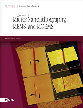
Journal of Micro/Nanolithography, MEMS, and MOEMS
VOL. 10 · NO. 4 | October 2011
CONTENTS
IN THIS ISSUE

Editorial (1)
Articles (17)
Errata (1)
Editorial
Journal of Micro/Nanolithography, MEMS, and MOEMS, Vol. 10, Issue 04, 040101, (October 2011) https://doi.org/10.1117/1.3665263
Open Access
TOPICS: Microelectromechanical systems, Microopto electromechanical systems, Microfabrication, Logic, Manufacturing, Optical lithography, Microsystems, Lithography, Semiconductors, Immersion lithography
JM3 Letters
Journal of Micro/Nanolithography, MEMS, and MOEMS, Vol. 10, Issue 04, 040501, (October 2011) https://doi.org/10.1117/1.3663567
Open Access
TOPICS: Fourier transforms, Stochastic processes, Metrology, Correlation function, 3D metrology, Lithography, 3D modeling, Spherical lenses, Data modeling, Line edge roughness
Articles
Tenghsien Lai, Chingfu Tsou
Journal of Micro/Nanolithography, MEMS, and MOEMS, Vol. 10, Issue 04, 043001, (October 2011) https://doi.org/10.1117/1.3641412
TOPICS: Microactuators, Electromagnetism, Magnetism, Packaging, Silicon, Nickel, Mirrors, Chemical oxygen iodine lasers, Thermal effects, Electroplating
Jalal Rouhi, Shahrom Mahmud, Sabar Hutagalung, Saeid Kakooei
Journal of Micro/Nanolithography, MEMS, and MOEMS, Vol. 10, Issue 04, 043002, (October 2011) https://doi.org/10.1117/1.3643480
TOPICS: Nanolithography, Electrodes, Scanning probe microscopy, Silicon, Photomasks, Oxides, Fabrication, Lithography, Transistors, Oxidation
Christopher Bencher, Jo Finders, Ilan Englard, Yaron Cohen, Amir Sagiv, Michael Ben-Yishai, Shmoolik Mangan, Huixiong Dai, Chris Ngai, Kfir Dotan, Roel Knops, Orion Mouraille, Evert Mos, Alexander Kremer
Journal of Micro/Nanolithography, MEMS, and MOEMS, Vol. 10, Issue 04, 043003, (October 2011) https://doi.org/10.1117/1.3641409
TOPICS: Photomasks, Semiconducting wafers, Critical dimension metrology, Lithography, Metrology, Inspection, Scanners, Optimization (mathematics), Double patterning technology, Wavefronts
Yiin-Kuen Fuh, Hung-Shuo Hsu
Journal of Micro/Nanolithography, MEMS, and MOEMS, Vol. 10, Issue 04, 043004, (October 2011) https://doi.org/10.1117/1.3644990
TOPICS: Nanofibers, Nanolithography, Near field, Polymers, Silicon, Fabrication, Atomic force microscopy, Plasma, Microfluidics, Liquids
Kosta Selinidis, Cynthia Brooks, Gary Doyle, Laura Brown, Chris Jones, Joseph Imhof, Dwayne LaBrake, Douglas Resnick, S. Sreenivasan
Journal of Micro/Nanolithography, MEMS, and MOEMS, Vol. 10, Issue 04, 043005, (October 2011) https://doi.org/10.1117/1.3646523
TOPICS: Photomasks, Chromium, Lithography, Etching, Electron beam lithography, Semiconductors, Semiconducting wafers, Inspection, Optical alignment, Silica
Journal of Micro/Nanolithography, MEMS, and MOEMS, Vol. 10, Issue 04, 043006, (October 2011) https://doi.org/10.1117/1.3644984
TOPICS: Photomasks, Inspection, Defect detection, Extreme ultraviolet, Wafer inspection, Semiconducting wafers, Defect inspection, Extreme ultraviolet lithography, Printing, Multilayers
Jeehong Yang, Serap Savari
Journal of Micro/Nanolithography, MEMS, and MOEMS, Vol. 10, Issue 04, 043007, (October 2011) https://doi.org/10.1117/1.3644620
Open Access
TOPICS: Image compression, Computer programming, Image processing, Binary data, Maskless lithography, Lithography, Metals, Electron beams, Direct write lithography, Photomasks
Journal of Micro/Nanolithography, MEMS, and MOEMS, Vol. 10, Issue 04, 043008, (October 2011) https://doi.org/10.1117/1.3658024
TOPICS: Nanoimprint lithography, Photomasks, Semiconductors, Lithography, Semiconducting wafers, Electron beam lithography, Optical lithography, Extreme ultraviolet lithography, Overlay metrology, Electron beams
Long-Fang Tsai, William Dahlquist, Seunghyun Kim, Gregory Nordin
Journal of Micro/Nanolithography, MEMS, and MOEMS, Vol. 10, Issue 04, 043009, (October 2011) https://doi.org/10.1117/1.3659139
TOPICS: Silicon, Microfluidics, Adhesives, Sensors, Ultraviolet radiation, Epoxies, Assembly equipment, Semiconducting wafers, Temperature metrology, Target detection
Andreas Brückner, Robert Leitel, Alexander Oberdörster, Peter Dannberg, Frank Wippermann, Andreas Bräuer
Journal of Micro/Nanolithography, MEMS, and MOEMS, Vol. 10, Issue 04, 043010, (October 2011) https://doi.org/10.1117/1.3659144
TOPICS: Wafer-level optics, Cameras, Modulation transfer functions, Channel projecting optics, Image sensors, Microlens array, Microlens, Semiconducting wafers, Image resolution, Prototyping
Jinseok Heo, Jeong-Ho Yeo, Young-Hee Kim
Journal of Micro/Nanolithography, MEMS, and MOEMS, Vol. 10, Issue 04, 043011, (October 2011) https://doi.org/10.1117/1.3658022
TOPICS: Scanners, Semiconducting wafers, Inspection, Calibration, Lithography, Image analysis, Spatial resolution, Scanning electron microscopy, Imaging systems, Overlay metrology
Journal of Micro/Nanolithography, MEMS, and MOEMS, Vol. 10, Issue 04, 043012, (October 2011) https://doi.org/10.1117/1.3659145
TOPICS: Cadmium, Semiconducting wafers, Computer simulations, Electron beams, Detection and tracking algorithms, Electron beam lithography, Point spread functions, Model-based design, Modulation, Nanoelectronics
Silvino Altuna, Adrian Fernandez, Miguel Garcia, Maria Rodriguez, Jose Rodriguez
Journal of Micro/Nanolithography, MEMS, and MOEMS, Vol. 10, Issue 04, 043013, (October 2011) https://doi.org/10.1117/1.3661993
TOPICS: Carbon, Photoresist materials, Manufacturing, Photomasks, Lithography, Electrodes, Glasses, Capillaries, Aluminum, Resistance
Jue-Chin Yu, Peichen Yu, Hsueh-Yung Chao
Journal of Micro/Nanolithography, MEMS, and MOEMS, Vol. 10, Issue 04, 043014, (October 2011) https://doi.org/10.1117/1.3663249
TOPICS: Photomasks, SRAF, Optical proximity correction, Wavefronts, Nanoimprint lithography, Lithography, Chaos, Image segmentation, Diffraction, Resolution enhancement technologies
Arun John Kadaksham, Thomas Laursen, Timothy Owen, Jon Underwood, Abbas Rastegar
Journal of Micro/Nanolithography, MEMS, and MOEMS, Vol. 10, Issue 04, 043015, (October 2011) https://doi.org/10.1117/1.3655725
TOPICS: Photomasks, Quartz, Monte Carlo methods, Extreme ultraviolet lithography, Scanning electron microscopy, Extreme ultraviolet, Multilayers, Electron beam lithography, Lithography, Inspection
Alok Vaid, Bin Bin Yan, Yun Tao Jiang, Mark Kelling, Carsten Hartig, John Allgair, Peter Ebersbach, Matthew Sendelbach, Narender Rana, Ahmad Katnani, Erin McLellan, Charles Archie, Cornel Bozdog, Helen Kim, Michael Sendler, Susan Ng, Boris Sherman, Boaz Brill, Igor Turovets, Ronen Urensky
Journal of Micro/Nanolithography, MEMS, and MOEMS, Vol. 10, Issue 04, 043016, (October 2011) https://doi.org/10.1117/1.3655726
TOPICS: Metrology, Scatterometry, Critical dimension metrology, Semiconducting wafers, Data modeling, Atomic force microscopy, Transmission electron microscopy, Inspection, 3D metrology
Chie Shishido, Maki Tanaka, Akira Hamamatsu, Tomoharu Nagao
Journal of Micro/Nanolithography, MEMS, and MOEMS, Vol. 10, Issue 04, 043017, (October 2011) https://doi.org/10.1117/1.3664410
TOPICS: Scanning electron microscopy, Model-based design, Monte Carlo methods, Calibration, Cadmium, Mathematical modeling, 3D metrology, Scatterometry, Semiconducting wafers, Metrology
COMMUNICATIONS
Yunqiao Wu, Jun Zhou, Edwin Pun
Journal of Micro/Nanolithography, MEMS, and MOEMS, Vol. 10, Issue 04, 049701, (October 2011) https://doi.org/10.1117/1.3665215
TOPICS: Liquids, Bioalcohols, Polymethylmethacrylate, Nanolithography, Capillaries, Silica, Fabrication, Scanning electron microscopy, Silicon, Image processing
Errata
Journal of Micro/Nanolithography, MEMS, and MOEMS, Vol. 10, Issue 04, 049801, (October 2011) https://doi.org/10.1117/1.3647513
Back to Top